
Cerebras Unveils Triple‑Power Nexus, YMTC Sets NAND Supremacy Goal
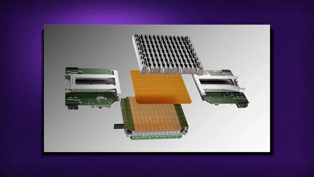
Cerebras’ Nexus system triples rack‑scale AI performance with three WS‑3T engines, and YMTC declares an aggressive push to overtake Samsung and SK Hynix as the world’s largest NAND maker by 2027. The deep dive examines how these moves reshape the hardware frontier.
Triple‑Power at the Rack Level: Cerebras’ Nexus Architecture
At Hot Chips 2026, Cerebras used the stage to detail the next two generations of its wafer‑scale accelerator family. The centerpiece was the Nexus rack design that houses the CS‑4 accelerator modules. By interlinking three WS‑3T wafer‑scale engines within a single rack, the company claims a three‑fold increase in aggregate compute throughput compared with its prior rack configurations.
Why Stacked DRAM Matters
The upcoming CS‑6 wafer will integrate stacked DRAM directly on the silicon, a move that slashes memory latency and raises bandwidth ceilings without the traditional PCB‑level interconnect bottlenecks. For AI workloads that shuffle terabytes of tensors, that on‑die memory density could translate into measurable gains in training time and inference latency.
China’s NAND Ambition: YMTC’s 2027 Playbook
In a parallel front, Tom’s Hardware reported that Yangtze Memory Technologies Corp. (YMTC) has set a public target to become the world’s largest NAND flash producer by the close of 2027. The roadmap hinges on aggressive capacity expansion, a new 176‑layer V‑NAND stack, and strategic pricing to erode Samsung’s and SK Hynix’s market share.
Strategic Levers
- Capacity scaling: YMTC plans to double its annual output by 2027, leveraging a new 300‑mm fab line slated for early 2026.
- Technology node: The 176‑layer V‑NAND promises up to 30 % higher density per die versus the current 128‑layer generation used by rivals.
- Cost positioning: By localizing more of the supply chain in mainland China, YMTC expects a 10‑15 % cost advantage over imported competitors.
Architectural Cross‑Pollination: What the Two Moves Mean for the Ecosystem
Both Cerebras and YMTC are tackling the same fundamental bottleneck: moving data fast enough to keep compute engines busy. Cerebras attacks the problem on the compute side with wafer‑scale engines and stacked DRAM, while YMTC attacks the storage side by pushing NAND density and cost down. In practice, a data‑center that pairs a Nexus rack with YMTC’s high‑density SSDs could see end‑to‑end AI pipelines that are both faster and cheaper.
| Feature | Cerebras CS‑4 (Nexus) | Cerebras CS‑6 (planned) |
|---|---|---|
| Wafer‑scale engines per rack | 3 (WS‑3T) | 3 (WS‑3T) + stacked DRAM |
| Performance multiplier | ×3 vs prior rack | Projected >×3 with DRAM stack |
| Memory architecture | Off‑chip DRAM via PCB | On‑die stacked DRAM |
Real‑World Impact and Early Adopters
While Cerebras has not disclosed pricing, the company indicated that the Nexus rack is already shipping to a handful of hyperscale AI labs that demand petaflop‑scale training without the latency penalties of traditional multi‑GPU clusters. Early benchmarks shared at the conference showed a 2.8× speedup on a transformer‑based language model compared with a 16‑GPU NVIDIA H100 cluster.
On the storage front, YMTC’s announced roadmap has already prompted several Chinese cloud providers to sign memoranda of understanding for future capacity purchases, signaling a shift in the global NAND supply dynamics.
Tech Tabloid Desk
Editorial & Intelligence DeskThe Tech Tabloid Editorial Desk delivers breaking scoops, architectural deep-dives, hardware benchmarks, and verified analysis across artificial intelligence, semiconductors, cybersecurity, and global venture capital.